
This installation guide is intended for the Super Famicom/SNES Jr. and covers capacitor replacement, as well as the simultaneous installation of the SNES RGB and SNES AIO. When installing both kits together, specific steps must be followed, as the process deviates from the original individual guides.
Please click here if you wish to purchase a capacitor kit, here if you wish to purchase a SNES RGB bypass kit or here if you wish to purchase a SNES AIO kit.
Contents
Please click below to skip to each section.
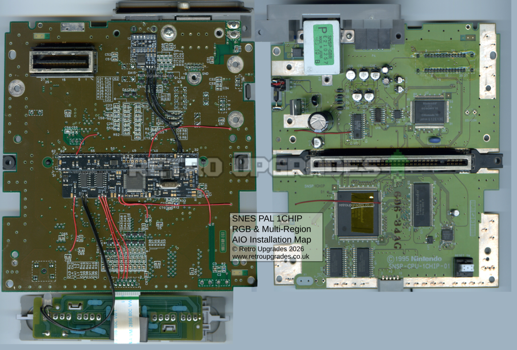
1.0 – Super Nintendo PAL 1CHIP (SNSP-CPU-1CHIP-01/02 Quick Install Map
2.0 – Full Installation Guide
2.1 – Capacitor Replacement
2.2 – SNES RGB Bypass
2.3.1 – SNES Multi-Region AIO Component Removal
2.3.2 – SNES Multi-Region AIO Installation of PCB
2.3.3 – SNES Multi-Region AIO Connections
2.3.4 – SNES Multi-Region AIO LED
2.3.5 – SNES Multi-Region AIO Jumpers
1.0 – Quick Install Map
Please click here for the full size image(opens in a new tab). Caution: large image file size. (Coming soon).
*This image is currently an example install. Quick install map is coming soon.
2.0 – Full Installation Guide
2.1 – Capacitor Replacement
We recommend starting off with the capacitor replacement if planned to ensure normal operation prior to installing any modification kits. If the capacitor kit is installed after installing the kits, it may make troubleshooting any potential future issues more bothersome.
Once the capacitors and voltage regulator have been replaced, test the console is working as expected before proceeding to the next section.
Optional: if your console experiences the vertical line issue, attach the 470uF/6.3V capacitor to the voltage regulator provided with your capacitor replacement kit. See here.
2.2 – SNES RGB Bypass
For this step, we’ll follow Tzorrimahm’s original guide here. We recommend following Tzorrimahm’s guide, but included below are a few pictures from our install.
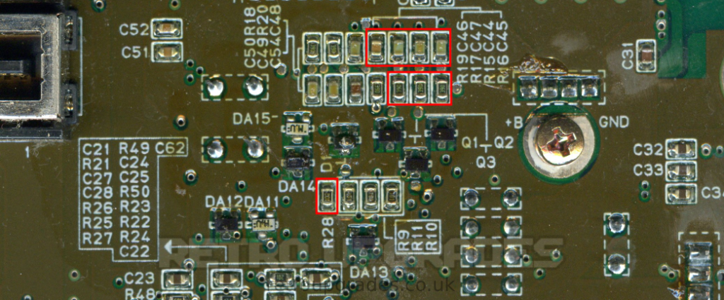
Disconnect +12V from MultiOut Pin 3: remove ‘R28‘.
Disconnect stock RGB: remove ‘R15’, ‘R16’, ‘R17‘.
Remove decoupling caps from MultiOut: remove ‘C44’, ‘C45’, ‘C46’, ‘C47‘.
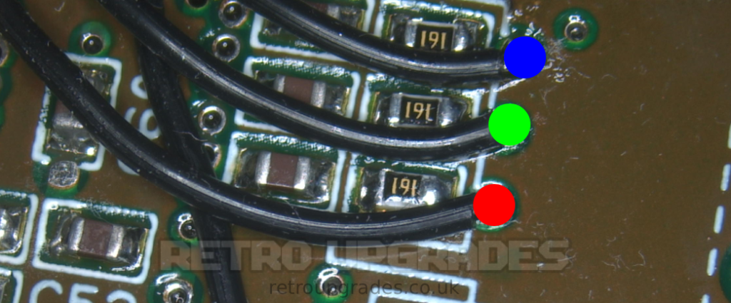
‘R’ on the SNES RGB bypass board to the right side of ‘R6’.
‘G’ on the SNES RGB bypass board to the right side of ‘R7’.
‘B’ on the SNES RGB bypass board to the left side of ‘R8’.
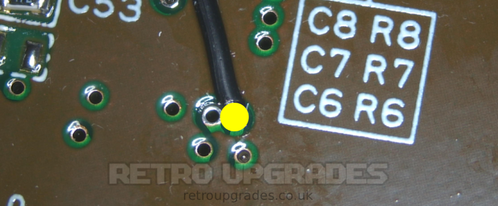
‘CS’ on the SNES RGB bypass board to the via highlighted. It is the via closest to silkscreen ‘C6’.
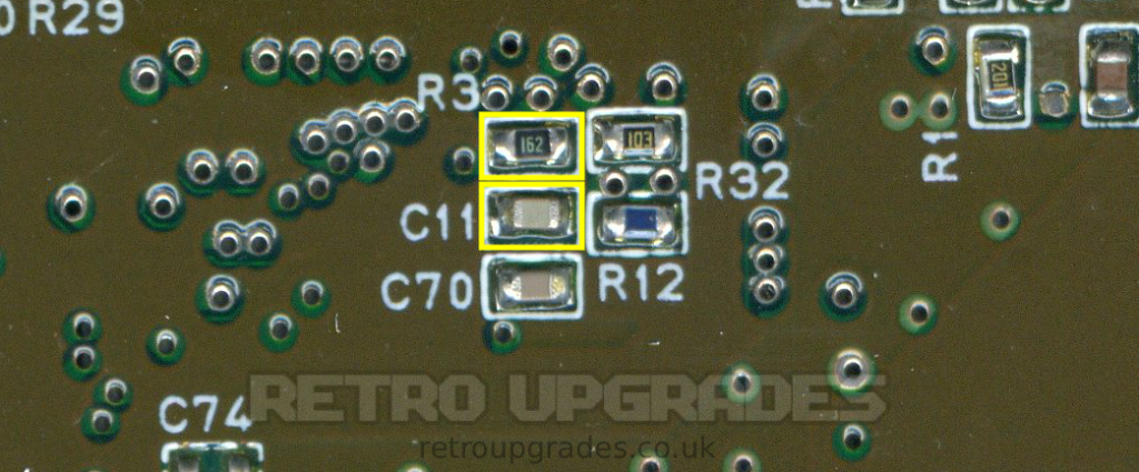
‘R3′ must be replaced with the brightness fix resistor included with the SNES RGB kit.
Optional: Replace ‘C11’ with the ghosting fix capacitor included with your SNES RGB kit. The console can be tested first and we only recommend to replace ‘C11’ if you are experiencing any ghosting.
Test the console to ensure operation is normal. The console should now output bypassed RGB.
2.3.1 – SNES Multi-region AIO – Component Removal
After successfully installing the SNES RGB kit, it’s time to prepare the board for the SNES AIO kit.
Lift pins 1, 2, 10 and 11 of CIC-lock ‘U8’. It is the small IC located next to the reset switch.
Optional: You can alternatively remove ‘U8’ if you find it easier than lifting pins (personal preference). If you remove ‘U8’, you can also remove ‘C9’.
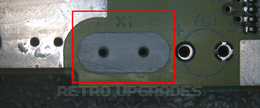
Remove X1.
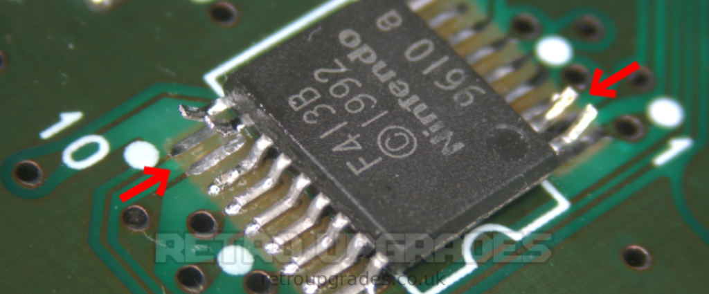
Lift S-CPUN pin 111.
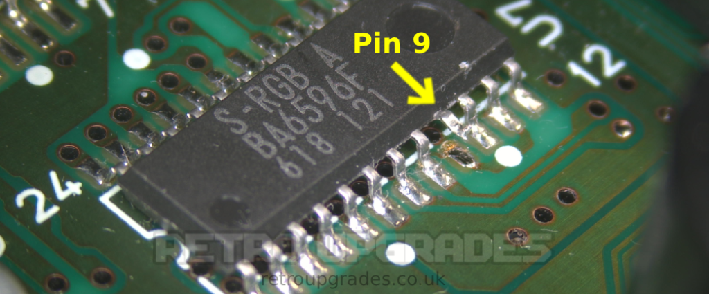
Lift S-RGB pin 9.
2.3.2 – SNES Multi-region AIO – Installation of the PCB
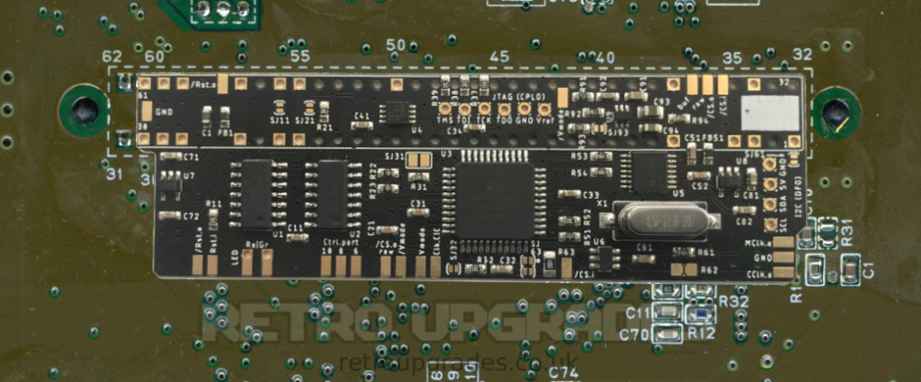
Align the AIO board to the cartridge slot pins on the bottom side of the SNES. The pin markings must match. Beware of orientation!
Ensure there is a small gap between the SNES mainboard and SNES AIO board. We slide a thin piece of card underneath the board prior to soldering. Alternatively, the bottom side of the AIO board can be isolated with tape prior to soldering.
Solder the PCB in place. Important: All connections must be well flowed. Pin ‘5’ and pin ’36’ may need more power due to the higher thermal mass of the GND plane.
2.3.3 – SNES Multi-region AIO – Connections
Please feel free to cross-reference with the quick install map as it provides a clear overview of the board.
(Coming soon). Click here for the quick install map (opens in a new tab). Caution: large image file size.
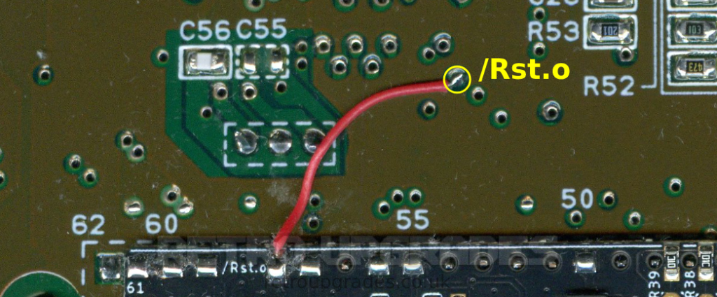
Connect the upper ‘Rst.o’ pad on the AIO board to the via highlighted above.
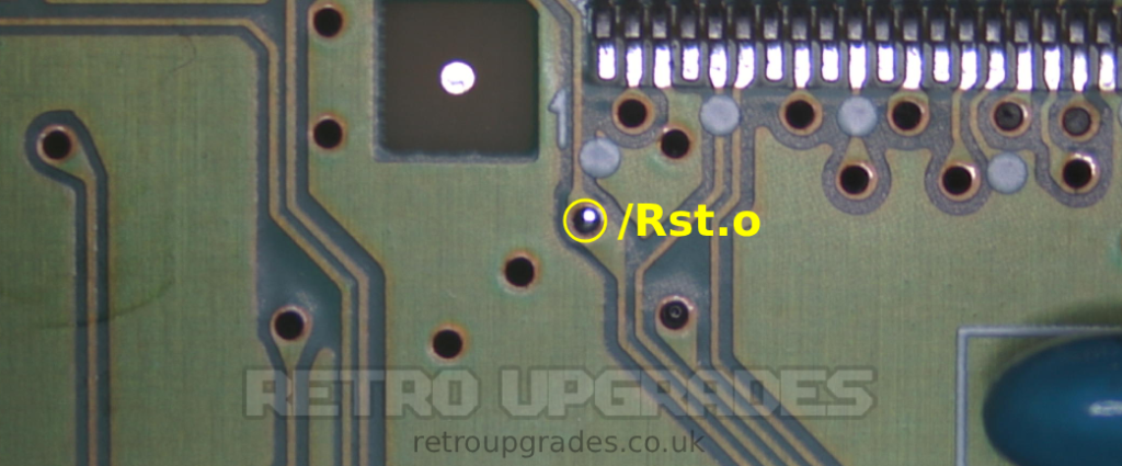
View of ‘Rst.o’ via from top side of the board. It is connected to S-APU pin 100 + CIC-lock pin 10.
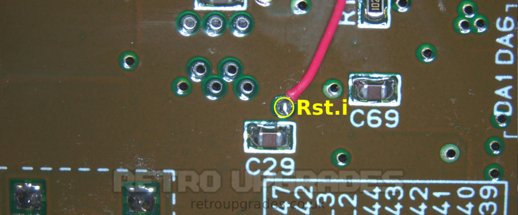
Connect the ‘Rst.i’ pad on the AIO board to the via immediately above ‘C29’ which is near the reset switch.
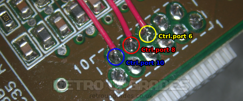
Connect the ‘Ctrl.port 10’ pad to pin ’10’ of the connector which attaches to the front panel controller board.
Connect the ‘Ctrl.port 8’ pad to pin ‘8’ of the connector which attaches to the front panel controller board.
Connect the ‘Ctrl.port 6’ pad to pin ‘6 of the connector which attaches to the front panel controller board.
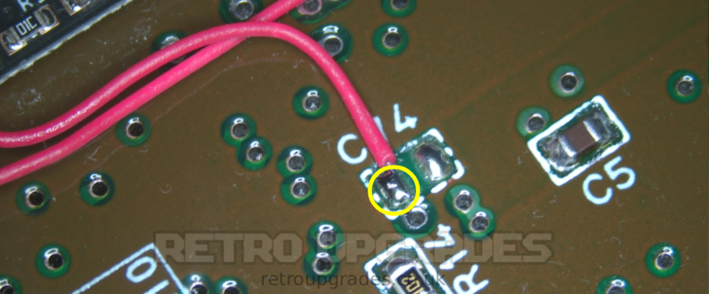
Connect ‘Clk.CIC’ pad which is center bottom of the AIO board to the left pad of ‘C74’. Alternatively: you can close jumper ‘SJ11’.
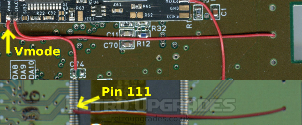
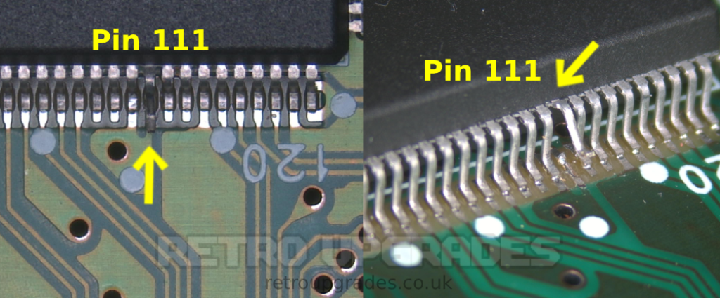
Our optimal wire routing for ‘Vmode’ to ‘Pin 111’.
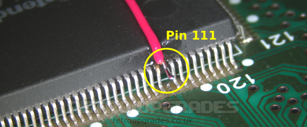
Connect the ‘Vmode’ pad (NOT /Vmode) on the AIO board to lifted pin 111 of the S-CPUN. Place some kapton tape on the top of S-CPUN to help act as strain relief.
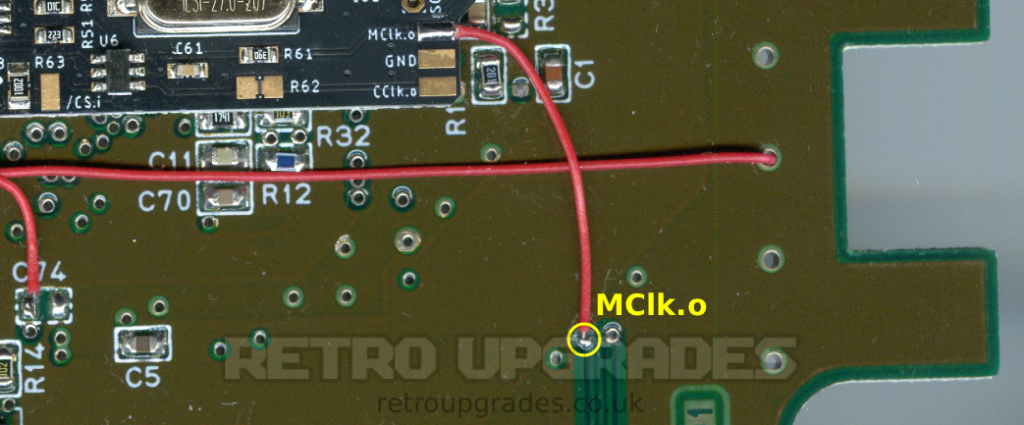
Connect ‘MCLK.o’ to the left via which connects to ‘X1’ (the side which connects to S-CPUN pin 9).

Remove the sync wire that connects the RGB bypass board to the via next to ‘C6’. (We previously connected this wire to ensure functionality of the RGB bypass board but now we’ll re-route sync).
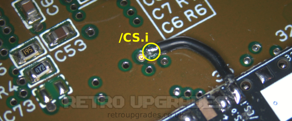
Connect ‘/CS.i’ (sync in) pad on the AIO board to the via closest to ‘C6’.
A view from the topside of the board of the via which should be connected to the ‘/CS.i’ pad of the AIO board. This via should have continuity between pin 7 of the S-RGB.
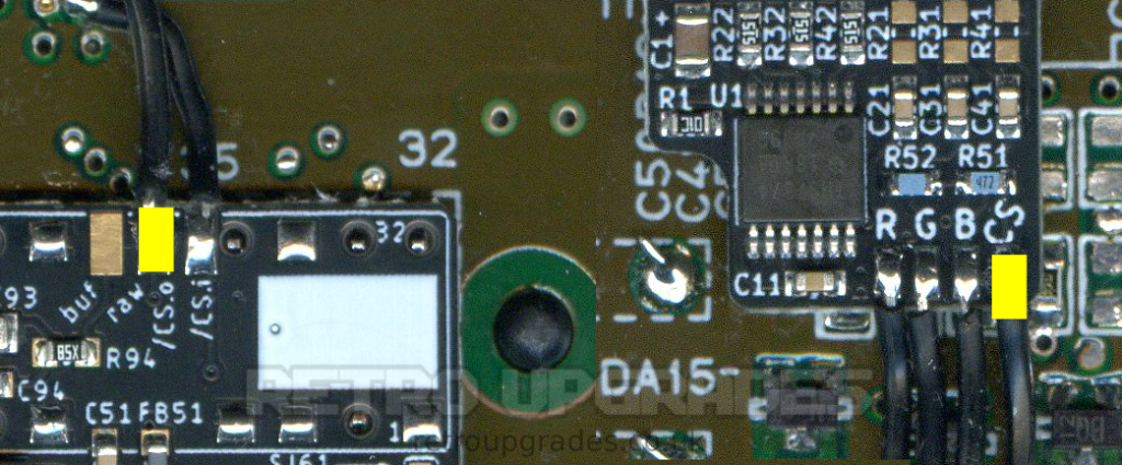
Connect the ‘/CS.o raw’ (TTL csync out) pad on the AIO board to the ‘CS’ pad on the SNES RGB board.
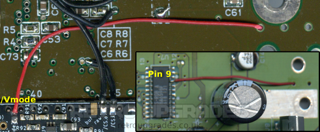
Our optimal wire routing for ‘/Vmode’ to S-RGB ‘Pin 9’.
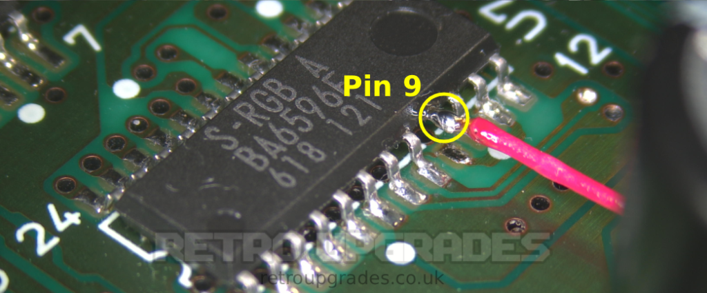
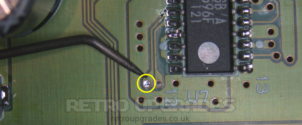
Connect the upper ‘/Vmode’ pad to lifted pin 9 of the S-RGB.
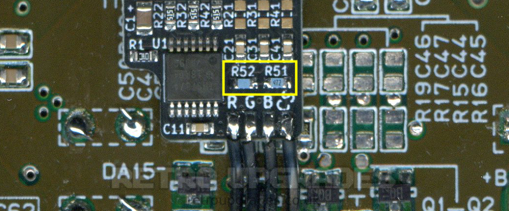
Lastly, when both kits are installed, two resistor values on the SNES RGB bypass board need to be changed. These resistors are included if both kits are purchased from us in the same order.
‘R51′ must be replaced with a ‘4.7kΩ 0603′ resistor.
‘R52′ must be replaced with a ‘10.7kΩ 0603’ resistor.
2.3.4 – SNES Multi-region AIO – LED
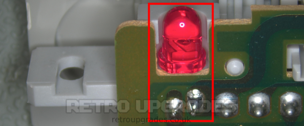
Remove the original LED from the front controller board panel.
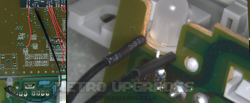
Connect the middle cathode pin of the supplied 3-pin LED to the ground (right side) pad on the controller board. The LED we supply is common cathode.
The two left and right pins of the LED can be wired to the two LED pads on the AIO board depending on which colour is desired per region selection. We have ours wired for red = 50Hz, blue = 60Hz, and purple = auto-select.
2.3.5 – SNES Multi-region AIO – Jumpers
We typically only adjust ‘SJ31’ which is Dejitter enable/disable. That’s it.
Optional: depending on your setup, you may wish to configure other jumpers.
- ‘SJ11’: Alternative clock for the SuperCIC. Close this jumper if you don’t connect the Clk.CIC pad in order to use the clock meant for the CIC key.
- ‘SJ21’: Close this jumper if you use an LED with a common anode. Otherwise, leave this jumper untouched.
- ‘SJ31’: Closing this jumper permanently disables the DeJitter function. This solder jumper is slightly larger to give the installer the option to connect a slide switch here (speed-runner discussions). We recommend keeping DeJitter off unless you are using the OSSC or are experiencing issues getting a stable picture.
- ‘SJ32’: Short this jumper if the board is installed in a non-1Chip SNES. (Note: SNES Jr. / SNES2 are also 1Chip models.)
- ‘SJ61’: Distributes clock output to cartridge slot pin 1. Do not close this jumper on 1Chip SNES units. Note: If SJ32 is open, SJ61 must also be open.
- ‘SJ63’: Determines which color carrier is forwarded to output. This jumper has two options. Do not close both!
- ‘SJ63.1’: (marked with a dot): Outputs color carrier derived from non-DeJittered clock. Use this if you experience discoloration on composite video or S-Video (see related discussion thread at shmups).
This is the default for all earlier versions of the mod board flashed with the current firmware. To use the other color carrier, revert to a previous firmware version. - ‘SJ63.2’: Outputs color carrier derived from the DeJittered clock. (We personally need to use this, as our TV does not like the color carrier from the non-DeJittered clock.)
Important: You must not close both jumpers! - ‘SJ93: Controls the sync level of buffered CSYNC output.
- Open: ~1.87V @ 75Ω termination (Most common).
Requires a resistor inside the sync wire to further attenuate the signal. Designed for cables with a 470Ω resistor, resulting in ~450mV @ 75Ω. - Closed: ~300mV @ 75Ω termination.
Suitable for pass-through wired sync cables. Works with standard TV/scaler setups.
RGB cables: NTSC SNES RGB SCART cables wired for CSYNC with a 470 ohm resistor on the sync line should be used. We disconnected +12V from pin 3 (CSYNC) during the RGB mod install which is why we can use this cable type on a PAL console. The RGB bypass is configured for use with this cable.
Troubleshooting:
If any noticeable flickering is present whilst using composite video or s-video, please see here for a fix or alternatively disable dejitter with ‘SJ31’.
When using an Everdrive, if there are a few lines missing from the top of the picture, it is due to the ghosting capactitor. Either adjust the value between 220nF-470nF or adjust the “1 CHIP transient fixes” setting in the Everdrive menu.